Difference between revisions of "PCB Design"
| Line 65: | Line 65: | ||
** Add a final rectangular polygon plane over the entire design and click Ratsnest - this helps to avoid board warping, better ground and signal conditions | ** Add a final rectangular polygon plane over the entire design and click Ratsnest - this helps to avoid board warping, better ground and signal conditions | ||
** To only see the board without the pour, use Ripup on the polygon | ** To only see the board without the pour, use Ripup on the polygon | ||
For further details, check this great resource: | |||
* [http://www.mbedded.ninja/pcb-design mbedded PCB design] | |||
== Board config == | == Board config == | ||
Revision as of 14:23, 5 August 2015
The the prototyping is done, putting the design proper PCB board makes it more rigid and possible to offer unassembled kits. The process is mostly straight forward but the design process to lay out the board requires some time to get right.
Eagle will be used here, it's cross platform and great part libraries.
Setup
- Eagle parts libraries:
- SparkFun Eagle Library
- Includes most of the parts SparkFun offer ont their website
- Adafruit Eagle Library
- Ladyada has made a library for most of the parts used in their tutorials
- SparkFun Eagle Library
- Altium libraries:
CAM
CAM, Computer Aided Manufacturing, to create processing files for fab houses.
- SparkFun sfe-gerb274x.cam CAM - Excellent generator of the necessary gerber and drill files, picks the right layers
- Creates the proper gerber files for manufacturing (highlighted are common for double-sided, one-sided silkscreen):
- GLT - Top copper layer, main traces
- GTS - Top soldermask, where to put tin/gold plated pads and mask all other green/other color
- GTO - Top silkscreen, all text, lines, illustrations can be painted on top of the soldermask
- GBL - Bottom copper layer, same bottom
- GBS - Bottom soldermask, same bottom
- GBO - Bottom silkscreen, same bottom
- GTP - Top solder paste stensil, only needed for SMD assembly of parts on the board
- TXT - NC type drill coordinates, for vias and mounting holes
Also, include a txt-file with specific fabrication instructions for the design. This helps to minimize confusion and wasted manufacturing time.
CAD Software
- Cadsoft Eagle PCB - Huge community support, loads of libraries, great for smaller boards, but feels a bit like the '80s
- Altium Designer - Industry standard, flexible, like Photoshop for electronics designers, quite expensive
- KiCad EDA - Open source multi-platform schematics and PCB layout software
- Viewplot - View the files coming out of Eagle for verification
Good practices
Some of these guidelines can be used in the Design Rules property window in Eagle. The PCB manufacturer normally provide a list of minimum requirements for their equipment/method.
Design rules:
- Clearances:
- Width: 10 mils / 0.254 mm - spacing between traces, pads, vias. Also same signal smd components, pads, vias - ground pour isolation can be set in polygon properties
- Distances:
- Board edge copper isolation: 12-50 mils / 0.3048-1.27 mm - for clean routing cut or v-score and avoiding shortcircuitings
- Drill and hole distance: 8 mils - minimum distance between drill holes
- Sizes:
- Min. width: 8 mils
- Board frame width: 8 mils - used for cutting and panelizing
- Signal trace width: 12-16 mils / 0.254-0.4064 mm - enough distance to avoid shortcircuiting of traces during fab
- Power trace width: 16-24 mils / 0.4064-0.6096 mm - allow large currents to flow in vcc and ground traces
- Min. drill size: 20 mils / 0.508 mm - minimum via and hole size, restricted by fab, use larger for better via-connections
- Min. width: 8 mils
- Restring for pads, vias:
- Percentage of drill size: 25% - enough surface to add solder
- Min. width: 12mils - minimum restring size
- Max. width: 20mils - maximum restring size
- Masks:
- Stop soldermask: 4 mils / 100% / 4 mils - Bleed a litt over the pad or via to make sure it's properly tinned
- Soldermask limit: 32 mils - little higher than the largest via to cover them with the mask instead of open tin/gold plating, aka. tented
Other:
- Labels and text:
- Add silkscreen labels to all connections and interfacing points
- Add a revision and date label
- Use vektor text, size 0.05 mils, and bold ratio 15%
- Ground pour:
- Add a final rectangular polygon plane over the entire design and click Ratsnest - this helps to avoid board warping, better ground and signal conditions
- To only see the board without the pour, use Ripup on the polygon
For further details, check this great resource:
Board config
- FR-4, FR-406, FR-408, FR-5, G10, CEM3, Rogers, ceramics - FR4 stands for Flame Retardant material made of woven glass reinforced epoxy resin
- Standard: FR4 1.6 mm thickness
- TG130, TG190, TG230 - Different temperature thresholds before the laminate begins to soften
- Standard: TG130
- 2/4/6/8 layers - Multiple signal, ground, and power layers
- Standard: 2 layers
- 0.5oz/1oz/2oz/3oz/4oz/5oz/6oz copper - Thickness top surface for traces and ground pour
- Standard: 1oz
- V-scoring / Tab-routing - Ways to separate boards from panels
- Standard: Both - V-scoring for square designs, tab for all other
- Surface finish - type of material added to exposed copper pads [1] [2]
- Standard: HASL / Immersion Silver
- HASL (Hot Air Solder Leveling) - 63/37 tin, standard, cheap, stress issues, uneven surface
- HASL Lead-free - not for fine pitch devices, RoHS compliant
- Immersion Tin - historically popular, flat surface 20-40 micron, 3-6 months shelf life
- ENIG (Electroless Nickel/Immersion Gold) - best for fine pitch devices, lead-free, 75 micron + 3-5 micron, excellent shelf-life
- Immersion Silver - lead-free, 5-12 micron, 12 months shelf-life, cost effective
- Hard Gold - expensive, long shelf-life, hard to solder to
Examples
These are some of the boards I've designed and got fabricated.
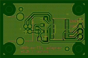
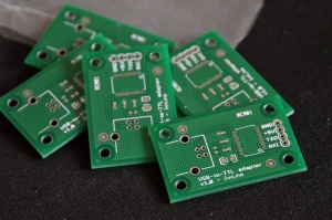
USB-to-TTL adapter
A small board I did for exploring Eagle
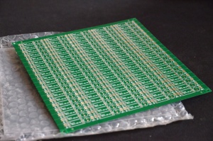
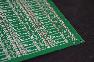
LC power filter
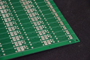
A compact and thin board (low-pass filter) panelized for easy PCB assembly.
PCB Manufacturers
A great place to start is Ladyada's PCB cost calculator. It lets you compare different manufacturers by cost per square inch. Note: Prices from 2007.
- BatchPCB - Easy and cheap for small boards
BatchPCB order
In mid-December 2010 I tried BatchPCB, a SparkFun service. Tried a sample board i designed. The result was satisfactory. I ordered 3 pieces but got 6 back, bonus! BatchPCB are putting multiple designs on a panel and shipping them to them to GoldPhoenixPCB. A small board including shipping is 15 USD, but the delivery time is 3 weeks.
Timeline:
- 2010-12-16 07:43:39 Submitted, passed, paid and pending
- 2010-12-17 07:12:18 Processing
- 2011-01-03 10:39:40 Shipped
- 2011-01-13 14:39:00 Arrived
This was during the xmas holidays and shipped from US to Norway, a normal turnaround would probably be 3 weeks.
GoldPhoenixPCB
Great for entire full panel runs with only a single board design, repeated. BatchPCB are using them. Based in Wuhan, China. Fast under 6 hour email response. Offers RoHS boards.
Small 36.4 L x 9.4 W x 0.8 H mm board, 200 pieces, one panel, order total 200USD inc. shipping.
First batch timeline:
- 2011-05-01 Design start
- 2011-05-06 Submitted and processed
- 2011-05-16 Final testing
- 2011-06-17 Shipped Fedex
- 2011-06-25 Arrived
Round-trip for a batch is around 3 weeks.
Second batch timeline:
- 2012-01-14 New run request sent
- 2012-01-19 Processed
- 2012-02-02 Tested and shipped Fedex
- 2012-02-07 Arrived
Round-trip for a batch is little over 3 weeks.
PCBCart
Haven't tried them yet. Eevblog are using them for uCurrent and uCalc.
Futurlec
Possible to order single or double sided boards, with or without soldermask or silkscreen. US based. Simple quotation form. A small board without silk or soldermask is 25 USD + shipping.
PCBTrain
UK based.
PCBPool
UK based.
DorkBotPDX
Batch run of boards, sent off when the board is full.
EzPCB
Low prices and value [3], offer prototyping and production services.
EuroCircuits
Based on Begium, good prices, proper web order system, fast delivery options. [4]
SeeedStudio
Chinese webstore offering PCB and laser cutting service, small 10pcs 5x5cm boards for 10USD, great for prototypes [5]. Quality of the received batch was great, no obvious issues, a small serial number was added to the boards by the manufacturer which is not that nice.
Small 28.5 L x 9.8 W x 0.8 H mm board, 11 pieces, order total 14.50USD inc. Airmail shipping.
Timeline:
- 2013-03-08 Submitted via web interface
- 2013-03-15 Shipped
- 2013-03-18 Traceable
- 2013-03-26 Delivered
Round-trip for this prototype batch was 18 days, pretty good. Faster shipping options are available so the shipping time can be cut down to 3-4 days.
Timeline Express shipping:
- 2013-09-02 Order placed
- 2013-09-06 Shipped
- 2013-09-08 Traceable
- 2013-09-11 Delivered
A turn-around time of 9 days using DHL express shipping, which is quite usable.
OSH Park / DorkBotPDX
- Great for prototype runs or small quantity. US based, same system as BatchPCB. Ships a full panel when it has filled up. Around 2USD for a small board, you get 3 pcs, 5USD international shipping.
DirtyPCBs
Very similar model to Seeed Studio where you pick a standard dimension set and quantity. Quality seems good going from these photos. Free shipping!
Smart Prototyping
Also offering a PCB service with several parametric, much like Seeed Studio. Can select whether to include a stencil, very handy.
PCB Stencil
To make SMD/SMT assembly easier and faster, get a PCB stencil to put solder paste directly on all the exposed solder pads. For more details, see Adafruit's SMT manufacturing guide.
Make sure to edit the top (or/and bottom) paste mask to remove any pads which should not have solder applied, e.g. jumper solder bridges, solder pads for wires, exposed areas, etc. In Altium, after exporting the Gerber files, it opens the Camtastic editor, used the Edit->Clear function to mark and right-click to delete, then Export->Gerber files to get the updated files.
Seeed Studio
Starting at 70USD you can get a 37x47cm laser cut stainless-steel stencil for full production runs/fabrication houses.
Ohararp Stencil
For small runs, Kapton stencil is cheap and works great for simple boards. Prepare the board outline (GKO) and top paste mask (GTP) gerber files and submit them using the easy ordering system. For 25USD+8USD shipping you can get a fairly large sheet, 215.9x279.4x0.0889mm (8.5″x11″x.0035″) - about the size of an A4 sheet.
OSH Stencil
Another good source. 0.30USD per square inch and low shipping cost.
PCB Penalization
Putting multiple board designs on a single PCB panel can save wasted material and speed for the assembler.
PCB Assembler
Gold Phoenix PCB
Professional PCB assembler, can manufacture the PCBs and part assembly.
Smart Prototyping
Great for small runs. Fast response via email and focus on getting it right. Can do part sourcing.
